- 您现在的位置:买卖IC网 > Sheet目录322 > DS2030Y-70# (Maxim Integrated)IC NVSRAM 256KBIT 70NS 256BGA
�� �
�
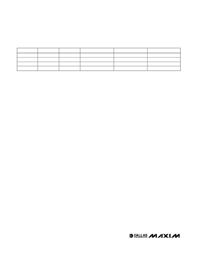
�DS2030Y/AB� Single-Piece� 256kb�
�Nonvolatile� SRAM�
�Memory� Operation� Truth� Table�
�WE�
�1�
�1�
�0�
�X�
�CE�
�0�
�0�
�0�
�1�
�OE�
�0�
�1�
�X�
�X�
�MODE�
�Read�
�Read�
�Write�
�Standby�
�I� CC�
�Active�
�Active�
�Active�
�Standby�
�OUTPUTS�
�Active�
�High� Impedance�
�High� Impedance�
�High� Impedance�
�X� =� Don’t� care.�
�Read� Mode�
�The� DS2030� executes� a� read� cycle� whenever� WE� (write�
�enable)� is� inactive� (high)� and� CE� (chip� enable)� is� active�
�(low).� The� unique� address� specified� by� the� 15� address�
�inputs� (A0� to� A14)� defines� which� of� the� 32,768� bytes� of�
�data� is� to� be� accessed.� Valid� data� will� be� available� to� the�
�eight� data� output� drivers� within� t� ACC� (access� time)� after�
�the� last� address� input� signal� is� stable,� providing� that� CE�
�and� OE� (output� enable)� access� times� are� also� satisfied.�
�If� CE� and� OE� access� times� are� not� satisfied,� then� data�
�access� must� be� measured� from� the� later� occurring� sig-�
�nal� (� CE� or� OE� )� and� the� limiting� parameter� is� either� t� CO� for�
�CE� or� t� OE� for� OE� rather� than� address� access.�
�Write� Mode�
�The� DS2030� executes� a� write� cycle� whenever� the� CE�
�and� WE� signals� are� active� (low)� after� address� inputs�
�are� stable.� The� later-occurring� falling� edge� of� CE� or� WE�
�will� determine� the� start� of� the� write� cycle.� The� write�
�cycle� is� terminated� by� the� earlier� rising� edge� of� CE� or�
�WE� .� All� address� inputs� must� be� kept� valid� throughout�
�the� write� cycle.� WE� must� return� to� the� high� state� for� a�
�minimum� recovery� time� (t� WR� )� before� another� cycle� can�
�be� initiated.� The� OE� control� signal� should� be� kept� inac-�
�tive� (high)� during� write� cycles� to� avoid� bus� contention.�
�However,� if� the� output� drivers� have� been� enabled� (� CE�
�and� OE� active)� then� WE� will� disable� the� outputs� in� t� ODW�
�from� its� falling� edge.�
�Data-Retention� Mode�
�The� DS2030AB� provides� full� functional� capability� for�
�V� CC� greater� than� 4.75V� and� write-protects� at� 4.5V.� The�
�DS2030Y� provides� full� functional� capability� for� V� CC�
�greater� than� 4.5V� and� write-protects� at� 4.25V.� Data� is�
�maintained� in� the� absence� of� V� CC� without� additional�
�support� circuitry.� The� NV� static� RAM� constantly� moni-�
�tors� V� CC� .� Should� the� supply� voltage� decay,� the� NV�
�SRAM� automatically� write-protects� itself.� All� inputs�
�become� “� don� ’� t� care� ”� ,� and� all� data� outputs� become� high�
�impedance.� As� V� CC� falls� below� approximately� 2.7V�
�(V� SW� ),� the� power-switching� circuit� connects� the� lithium�
�energy� source� to� the� RAM� to� retain� data.� During� power-�
�up,� when� V� CC� rises� above� V� SW� ,� the� power-switching�
�circuit� connects� external� V� CC� to� the� RAM� and� discon-�
�nects� the� lithium� energy� source.� Normal� RAM� operation�
�can� resume� after� V� CC� exceeds� V� TP� for� a� minimum�
�duration� of� t� REC� .�
�Battery� Charging�
�When� V� CC� is� greater� than� V� TP� ,� an� internal� regulator�
�charges� the� battery.� The� UL-approved� charger� circuit�
�includes� short-circuit� protection� and� a� temperature-sta-�
�bilized� voltage� reference� for� on-demand� charging� of�
�the� internal� battery.� Typical� data-retention� expectations�
�of� 3� years� per� charge� cycle� are� achievable.�
�A� maximum� of� 96� hours� of� charging� time� is� required� to�
�fully� charge� a� depleted� battery.�
�System� Power� Monitoring�
�When� the� external� V� CC� supply� falls� below� the� selected�
�out-of-tolerance� trip� point,� the� output� RST� is� forced�
�active� (low).� Once� active,� the� RST� is� held� active� until�
�the� V� CC� supply� has� fallen� below� that� of� the� internal� bat-�
�tery.� On� power-up,� the� RST� output� is� held� active� until�
�the� external� supply� is� greater� than� the� selected� trip�
�point� and� one� reset� timeout� period� (t� RPU� )� has� elapsed.�
�This� is� sufficiently� longer� than� t� REC� to� ensure� that� the�
�SRAM� is� ready� for� access� by� the� microprocessor.�
�Freshness� Seal� and� Shipping�
�The� DS2030� is� shipped� from� Dallas� Semiconductor� with�
�the� lithium� battery� electrically� disconnected,� guarantee-�
�ing� that� no� battery� capacity� has� been� consumed� during�
�transit� or� storage.� As� shipped,� the� lithium� battery� is�
�~60%� charged,� and� no� preassembly� charging� opera-�
�tions� should� be� attempted.�
�When� V� CC� is� first� applied� at� a� level� greater� than� V� TP� ,�
�the� lithium� battery� is� enabled� for� backup� operation.� A�
�96� hour� initial� battery� charge� time� is� recommended� for�
�new� system� installations.�
�10�
�____________________________________________________________________�
�发布紧急采购,3分钟左右您将得到回复。
相关PDF资料
DS2045L-100#
IC NVSRAM 1MBIT 100NS 256BGA
DS2045W-100#
IC NVSRAM 1MBIT 100NS 256BGA
DS2045Y-70#
IC NVSRAM 1MBIT 70NS 256BGA
DS2050W-100#
IC NVSRAM 4MBIT 100NS 256BGA
DS2065W-100#
IC NVSRAM 8MBIT 100NS 256BGA
DS2070W-100#
IC NVSRAM 16MBIT 100NS 256BGA
DS2227-070
IC NVSRAM 4MBIT 70NS 72SIMM
DS2423D/T&R
IC SRAM 4KBIT 6FCHIP
相关代理商/技术参数
DS203A
制造商:C&K Components 功能描述:SWITCH SNAP ACTION 制造商:C&K Components 功能描述:DS203A / Alt#: HADS0011 / Series: COMAX
DS203MAC-B10/0,03
制造商:ABB Low Voltage Products and Systems 功能描述:System Pro M RCBO DS203 M AC-B10/0,03
DS203MAC-B16/0,03
制造商:ABB Control 功能描述:System Pro M RCBO DS203 M AC-B16/0,03
DS203MAC-B20/0,03
制造商:ABB Control 功能描述:System Pro M RCBO DS203 M AC-B20/0,03
DS203MAC-B25/0,03
制造商:ABB Control 功能描述:System Pro M RCBO DS203 M AC-B25/0,03
DS203MAC-B32/0,03
制造商:ABB Control 功能描述:System Pro M RCBO DS203 M AC-B32/0,03
DS203MAC-B40/0,03
制造商:ABB Control 功能描述:System Pro M RCBO DS203 M AC-B40/0,03
DS203MAC-B50/0,03
制造商:ABB Low Voltage Products and Systems 功能描述:System Pro M RCBO DS203 M AC-B50/0,03